ADDER & FLIP FLOP
ADDER & FLIP-FLOP
Adder
There are two adder half adder, full adder
Half Adder
Half adder is a circuit that will add two bits & produce a sum & a carry bit. It needs two input bits & two output bits.
Ex-OR gate will only produce an output “1” when “EITHER” input is at logic “1”, so we need an additional output to produce a carry output, “1” when “BOTH” inputs “A” and “B” are at logic “1” and a standard AND Gate fits the bill nicely.
By combining the Ex-OR gate with the AND gate results in a simple digital binary adder circuit known commonly as the “Half Adder” circuit.
Full Adder
A half adder has only two inputs & there is no provision to add a carry coming from the lower order bits when multi addition is performed.
For this purpose, a full adder is designed.
The 1-bit Full Adder circuit is basically two half adders connected together and consists of three Ex-OR gates, two AND gates and an OR gate, six logic gates in total.
The truth table for the full adder includes an additional column to take into account the Carry-in input as well as the summed output and carry-output.
Figure: Logic diagram of a Full adder using two Half Adders
Table: Truth Table for Full Adder
FLIP FLOP
RS Flip Flop
RS Flip Flop have two inputs, S and R. S is called set and R is called reset.
The S input is used to produce HIGH on Q ( i.e. store binary 1 in flip-flop).
The R input is used to produce LOW on Q (i.e. store binary 0 in flip-flop). Q’ is Q complementary output, so it always holds the opposite value of Q.
The output of the S-R Flip Flop depends on current as well as previous inputs or state, and its state (value stored) can change as soon as its inputs change.
The circuit and the truth table of RS Flip Flop is shown below.
The operation has to be analyzed with the 4 inputs combinations together with the 2 possible previous states.
When S = 0 and R = 0: If we assume Q = 1 and Q’ = 0 as initial condition, then output Q after input is applied would be Q = (R + Q’)’ = 1 and Q’ = (S + Q)’ = 0.
Assuming Q = 0 and Q’ = 1 as initial condition, then output Q after the input applied would be Q = (R + Q’)’ = 0 and Q’ = (S + Q)’ = 1.
So it is clear that when both S and R inputs are LOW, the output is retained as before the application of inputs. (i.e. there is no state change).
When S = 1 and R = 0: If we assume Q = 1 and Q’ = 0 as initial condition, then output Q after input is applied would be Q = (R + Q’)’ = 1 and Q’ = (S + Q)’ = 0.
Assuming Q = 0 and Q’ = 1 as initial condition, then output Q after the input applied would be Q = (R + Q’)’ = 1 and Q’ = (S + Q)’ = 0. So in simple words when S is HIGH and R is LOW, output Q is HIGH.
When S = 0 and R = 1: If we assume Q = 1 and Q’ = 0 as initial condition, then output Q after input is applied would be Q = (R + Q’)’ = 0 and Q’ = (S + Q)’ = 1.
Assuming Q = 0 and Q’ = 1 as initial condition, then output Q after the input applied would be Q = (R + Q’)’ = 0 and Q’ = (S + Q)’ = 1.
So in simple words when S is LOW and R is HIGH, output Q is LOW.
When S = 1 and R =1 : No matter what state Q and Q’ are in, application of 1 at input of NOR gate always results in 0 at output of NOR gate, which results in both Q and Q’ set to LOW (i.e. Q = Q’). LOW in both the outputs basically is wrong, so this case is invalid.
It is possible to construct the RS Flip Flop using NAND gates (of course as seen in Logic gates section).
The only difference is that NAND is NOR gate dual form (Did I say that in Logic gates section?).
So in this case the R = 0 and S = 0 case becomes the invalid case. The circuit and Truth table of RS Flip Flop using NAND is shown below.
If you look closely, there is no control signal, so this kind of Flip Flopes or flip-flops are called asynchronous logic elements.
Since all the sequential circuits are built around the RS Flip Flop, we will concentrate on synchronous circuits and not on asynchronous circuits.
RS Flip Flop with Clock
We have seen this circuit earlier with two possible input configurations: one with level sensitive input and one with edge sensitive input.
The circuit below shows the level sensitive RS Flip Flop. Control signal “Enable” E is used to gate the input S and R to the RS Flip Flop.
When Enable E is HIGH, both the AND gates act as buffers and thus R and S appears at the RS Flip Flop input and it functions like a normal RS Flip Flop.
When Enable E is LOW, it drives LOW to both inputs of RS Flip Flop. As we saw in previous page, when both inputs of a NOR Flip Flop are low, values are retained (i.e. the output does not change).
Set up and Hold time
For synchronous flip-flops, we have special requirements for the inputs with respect to clock signal input. They are
Setup Time: Minimum time period during which data must be stable before the clock makes a valid transition.
For example, for a posedge triggered flip-flop, with a setup time of 2 ns, Input Data (i.e. R and S in the case of RS flip-flop) should be stable for at least 2 ns before clock makes transition from 0 to 1.
Hold Time: Minimum time period during which data must be stable after the clock has made a valid transition.
For example, for a posed triggered flip-flop, with a hold time of 1 ns. Input Data (i.e. R and S in the case of RS flip-flop) should be stable for at least 1 ns after clock has made transition from 0 to 1.
If data makes transition within this setup window and before the hold window, then the flip-flop output is not predictable, and flip-flop enters what is known as meta stable state.
In this state flip-flop output oscillates between 0 and 1.
It takes some time for the flip-flop to settle down.
The whole process is called Meta stability.
You could refer to tidbits section to know more information on this topic.
The waveform below shows input S (R is not shown), and CLK and output Q (Q’ is not shown) for a SR posed flip-flop.
Figure: Waveform for S-R and CLK
D Flip Flop
The RS Flip Flop seen earlier contains ambiguous state; to eliminate this condition we can ensure that S and R are never equal.
This is done by connecting S and R together with an inverter.
Thus we have D Flip Flop: the same as the RS Flip Flop, with the only difference that there is only one input, instead of two (R and S).
This input is called D or Data input. D Flip Flop is called D transparent Flip Flop for the reasons explained earlier.
Delay flip-flop or delay latch is another name used. Below is the truth table and circuit of D Flip Flop.
In real world designs (ASIC/FPGA Designs) only D latches/Flip-Flops are used.
Figure 2.12: D Flip Flop with Edge Sensitive and Level sensitive
Table: Truth table for D Flip Flop
Below is the D Flip Flop waveform, which is similar to the RS Flip Flop one, but with R removed.
Figure: D Flip Flop waveform
JK Flip Flop
The ambiguous state output in the RS Flip Flop was eliminated in the D Flip Flop by joining the inputs with an inverter.
But the D Flip Flop has a single input. JK Flip Flop is similar to RS Flip Flop in that it has 2 inputs J and K as shown Figurer below.
The ambiguous state has been eliminated here: when both inputs are high, output toggles.
The only difference we see here is output feedback to inputs, which is not there in the RS Flip Flop.
T Flip Flop
When the two inputs of JK Flip-Flop are shorted, a T Flip-Flop is formed. It is called T Flip-Flop as, when input is held HIGH, output toggles.
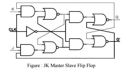
JK Master Slave Flip-Flop
All sequential circuits that we have seen in the last few pages have a problem (All level sensitive sequential circuits have this problem).
Before the enable input changes state from HIGH to LOW (assuming HIGH is ON and LOW is OFF state), if inputs changes, then another state transition occurs for the same enable pulse.
This sort of multiple transition problem is called racing.
If we make the sequential element sensitive to edges, instead of levels, we can overcome this problem, as input is evaluated only during enable/clock edges.
Figure: JK Master Slave Flip-Flop
In the Figure above there are two Flip Flop, the first Flip-Flop on the left is called master Flip Flop and the one on the right is called slave Flip Flop.
Master Flip Flop is positively clocked and slave Flip Flop is negatively clocked.
For more details about ADDER Click here
To see other topics in Basic Electrical and Electronics Engineering Click here
Click Here to Download the pdf of this topic ADDER
Other links
Bipolar Junction Transistor(BJT)
Binary Number System and Conversion
 Voltage Regulation: