Hexadecimal Numbers
In addition to binary, another number base that is commonly used in digital systems is base 16.
This number system is called hexadecimal, and each digit position represents a power of 16.
For any number base greater than ten, a problem occurs because there are more than ten symbols needed to represent the numerals for that number base.
It is customary in these cases to use the ten decimal numerals followed by the letters of the alphabet beginning with A to provide the needed numerals.
Since the hexadecimal system is base 16, there are sixteen numerals required.
The following are the hexadecimal numerals:
0, 1, 2, 3, 4, 5, 6, 7, 8, 9, A, B, C, D, E, F
The following are some examples of hexadecimal numbers:
1016 4716 3FA16 A03F16
The reason for the common use of hexadecimal numbers is the relationship between the numbers 2 and 16.
Sixteen is a power of 2 (16 = 24).
Because of this relationship, four digits in a binary number can be represented with a single hexadecimal digit.
This makes conversion between binary and hexadecimal numbers very easy, and hexadecimal can be used to write large binary numbers with much fewer digits.
When working with large digital systems, such as computers, it is common to find binary numbers with 8, 16 and even 32 digits. Writing a 16 or 32 bit binary number would be quite tedious and error prone.
By using hexadecimal, the numbers can be written with fewer digits and much less likelihood of error.
To convert a binary number to hexadecimal, divide it into groups of four digits starting with the rightmost digit.
If the number of digits isn’t a multiple of 4, prefix the number with 0’s so that each group contains 4 digits.
For each four digit group, convert the 4 bit binary number into an equivalent hexadecimal digit.
See the Binary, BCD, and Hexadecimal Number Tables at the end of this document for the correspondence between 4 bit binary patterns and hexadecimal digits.
Convert the binary number 10110101 to a hexadecimal number
To convert a hexadecimal number to a binary number, convert each hexadecimal digit into a group of 4 binary digits.
Convert the hex number 374F into binary
There are several ways in common use to specify that a given number is in hexadecimal representation rather than some other radix.
In cases where the context makes it absolutely clear that numbers are represented in hexadecimal, no indicator is used.
Written material where the context doesn’t make it clear what the radix is, the numeric subscript 16 following the hexadecimal number is used.
Programming languages, this method isn’t really feasible, so there are several conventions used depending on the language.
In the C and C++ languages, hexadecimal constants are represented with a ‘0x’ preceding the number, as in: 0x317F, or 0x1234, or 0xAF.
In assembler programming languages that follow the Intel style, a hexadecimal constant begins with a numeric character (so that the assembler can distinguish it from a variable name), a leading ‘0’ being used if necessary.
The letter ‘h’ is then suffixed onto the number to inform the assembler that it is a hexadecimal constant. In Intel style assembler format: 371Fh and 0FABCh are valid hexadecimal constants. Note that: A37h isn’t a valid hexadecimal constant.
It doesn’t begin with a numeric character, and so will be taken by the assembler as a variable name.
In assembler programming languages that follow the Motorola style, hexadecimal constants begin with a ‘$’ character.
So in this case: $371F or $FABC or $01 are valid hexadecimal constants.
Binary Coded Decimal Numbers
Another number system that is encountered occasionally is Binary Coded Decimal.
In this system, numbers are represented in a decimal form, however each decimal digit is encoded using a four bit binary number.
The decimal number 136 would be represented in BCD as follows: 136 = 0001 0011 0110
1 3 6
Conversion of numbers between decimal and BCD is quite simple.
To convert from decimal to BCD, simply write down the four bit binary pattern for each decimal digit.
To convert from BCD to decimal, divide the number into groups of 4 bits and write down the corresponding decimal digit for each 4 bit group.
There are a couple of variations on the BCD representation, namely packed and unpacked.
An unpacked BCD number has only a single decimal digit stored in each data byte.
In this case, the decimal digit will be in the low four bits and the upper 4 bits of the byte will be 0.
In the packed BCD representation, two decimal digits are placed in each byte.
Generally, the high order bits of the data byte contain the more significant decimal digit.
The following is a 16 bit number encoded in packed BCD format:
01010110 10010011
This is converted to a decimal number as follows: 0101 0110 1001 0011
5 6 9 3 The value is 5693 decimal
The same number in unpacked BCD (requires 32 bits)
00000101 00000110 00001001 00000011
5 6 9 3
The use of BCD to represent numbers isn’t as common as binary in most computer systems, as it is not as space efficient.
In packed BCD, only 10 of the 16 possible bit patterns in each 4 bit unit are used. In unpacked BCD, only 10 of the 256 possible bit patterns in each byte are used.
A 16 bit quantity can represent the range 0-65535 in binary, 0-9999 in packed BCD and only 0-99 in unpacked BCD.
Fixed Precision and Overflow
we haven’t considered the maximum size of the number. We have assumed that as many bits are available as needed to represent the number.
In most computer systems, this isn’t the case. Numbers in computers are typically represented using a fixed number of bits.
These sizes are typically 8 bits, 16 bits, 32 bits, 64 bits and 80 bits.
These sizes are generally a multiple of 8, as most computer memories are organized on an 8 bit byte basis.
Numbers in which a specific number of bits are used to represent the value are called fixed precision numbers.
When a specific number of bits are used to represent a number, that determines the range of possible values that can be represented.
For example, there are 256 possible combinations of 8 bits, therefore an 8 bit number can represent 256 distinct numeric values and the range is typically considered to be 0-255.
Any number larger than 255 can’t be represented using 8 bits. Similarly, 16 bits allows a range of 0-65535.
When fixed precision numbers are used, (as they are in virtually all computer calculations) the concept of overflow must be considered.
An overflow occurs when the result of a calculation can’t be represented with the number of bits available.
For example when adding the two eight bit quantities: 150 + 170, the result is 320.
This is outside the range 0-255, and so the result can’t be represented using 8 bits.
The result has overflowed the available range.
When overflow occurs, the low order bits of the result will remain valid, but the high order bits will be lost.
This results in a value that is significantly smaller than the correct result.
When doing fixed precision arithmetic (which all computer arithmetic involves) it is necessary to be conscious of the possibility of overflow in the calculations.
Signed and Unsigned Numbers
we have only considered positive values for binary numbers.
When a fixed precision binary number is used to hold only positive values, it is said to be unsigned.
In this case, the range of positive values that can be represented is 0 — 2n-1, where n is the number of bits used.
It is also possible to represent signed (negative as well as positive) numbers in binary.
In this case, part of the total range of values is used to represent positive values, and the rest of the range is used to represent negative values.
There are several ways that signed numbers can be represented in binary, but the most common representation used today is called two’s complement.
The term two’s complement is somewhat ambiguous, in that it is used in two different ways.
First, as a representation, two’s complement is a way of interpreting and assigning meaning to a bit pattern contained in a fixed precision binary quantity.
Second, the term two’s complement is also used to refer to an operation that can be performed on the bits of a binary quantity.
As an operation, the two’s complement of a number is formed by inverting all of the bits and adding 1.
In a binary number being interpreted using the two’s complement representation, the high order bit of the number indicates the sign.
If the sign bit is 0, the number is positive, and if the sign bit is 1, the number is negative.
For positive numbers, the rest of the bits hold the true magnitude of the number.
For negative numbers, the lower order bits hold the complement (or bitwise inverse) of the magnitude of the number.
It is important to note that two’s complement representation can only be applied to fixed precision quantities, that is, quantities where there are a set number of bits.
Two’s complement representation is used because it reduces the complexity of the hardware in the arithmetic-logic unit of a computer’s CPU.
Using a two’s complement representation, all of the arithmetic operations can be performed by the same hardware whether the numbers are considered to be unsigned or signed.
The bit operations performed are identical, the difference comes from the interpretation of the bits.
The interpretation of the value will be different depending on whether the value is considered to be unsigned or signed.
Find the 2’s complement of the following 8 bit number
The 2’s complement of 00101001 is 11010111
Find the 2’s complement of the following 8 bit number 10110101
The 2’s complement of 10110101 is 01001011
The counting sequence for an eight bit binary value using 2’s complement representation appears as follows:
Counting up from 0, when 127 is reached, the next binary pattern in the sequence corresponds to -128.
The values jump from the greatest positive number to the greatest negative number, but that the sequence is as expected after that. (i.e. adding 1 to –128 yields –127, and so on.).
When the count has progressed to 0FFh (or the largest unsigned magnitude possible) the count wraps around to 0. (i.e. adding 1 to –1 yields 0).
For more details about classification of Hexadecimal Numbers Click here
To see other topics in Basic Electrical and Electronics Engineering Click here
Click Here to Download the pdf of this topic Hexadecimal Numbers
Other links
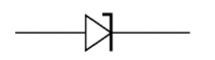
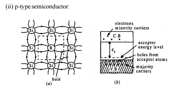
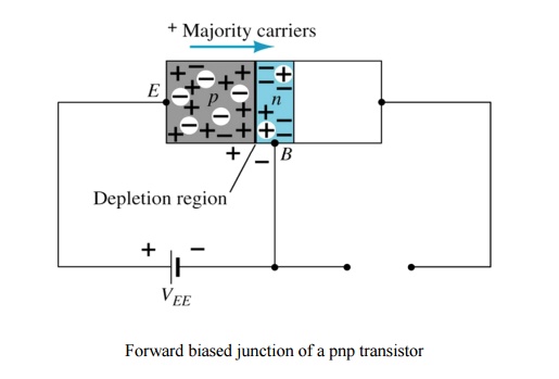
Bipolar Junction Transistor(BJT)
Binary Number System and Conversion
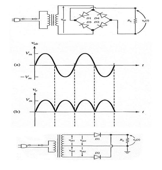 Voltage Regulation: